 | –≠–ª–µ–∫—Ç—Ä–æ–Ω–Ω—ã–π –∫–æ–º–ø–æ–Ω–µ–Ω—Ç: USB97C223 | –°–∫–∞—á–∞—Ç—å:  PDF PDF  ZIP ZIP |
SMSC USB97C223
Page 1
Revision 1.4 (08-27-03)
DATASHEET
USB97C223
Bus Powered USB
2.0 Flash Media Controller
Datasheet
Product Features
Complete System Solution for interfacing
SmartMedia
TM
(SM), Memory Stick
TM
(MS), High
Speed Memory Stick (HSMS), Memory Stick
PRO (MSPRO), Secure Digital (SD),
MultiMediaCard
TM
(MMC), NAND Flash, Compact
Flash
TM
(CF) and CF form-factor ATA hard drives
to USB 2.0 bus
- Supports USB Bulk Only Mass Storage Compliant
Bootable BIOS
Support for simultaneous operation of all above
devices. (only one at a time of each of the
following groups supported: CF or ATA drive, SM
or XD or NAND, SD or MMC)
On-Chip 4-Bit High Speed Memory Stick and MS
PRO Hardware Circuitry
On-Chip firmware reads and writes High Speed
Memory Stick and MS PRO
USB Bus Power Certified
3.3 Volt I/O with 5V input tolerance
Complete USB Specification 2.0 Compatibility for
Bus Powered Operation
- Includes USB 2.0 Transceiver
- A Bi-directional Control and a Bi-directional Bulk
Endpoint are provided.
8051 8 bit microprocessor
- Provides low speed control functions
- 30 Mhz execution speed at 4 cycles per instruction
average
- 12K Bytes of internal SRAM for general purpose
scratchpad
- 768 Bytes of internal SRAM for general purpose
scratchpad or program execution while re-flashing
external ROM
Double Buffered Bulk Endpoint
- Bi-directional 512 Byte Buffer for Bulk Endpoint
- 64 Byte RX Control Endpoint Buffer
- 64 Byte TX Control Endpoint Buffer
Internal or External Program Memory Interface
- 64K Byte Internal Code Space or Optional 64K Byte
External Code Space using Flash, SRAM or EPROM
memory.
On Board 12Mhz Crystal Driver Circuit
On-Chip 1.8V Regulator for Low Power Core
Operation
Internal PLL for 480Mhz USB2.0 Sampling,
Configurable MCU clock
Supports firmware upgrade via USB bus if "boot
block" Flash program memory is used
15 GPIOs for special function use: LED
indicators, button inputs, power control to
memory devices, etc.
- Inputs capable of generating interrupts with either
edge sensitivity
Compatible with Microsoft WinXP, WinME,
Win2K SP3, Apple OS10 and Linux Multi-LUN
Mass Storage Class Drivers
Win2K, Win98/98SE and Apple OS8.6 and OS9
Multi-LUN Mass Storage Class Drivers available
from SMSC
128 Pin TQFP Package (1.0mm height, 14mm
x14mm footprint)
Bus Powered USB 2.0 Flash Media Controller
Datasheet
Revision 1.4 (08-27-03)
Page 2
SMSC USB97C223
DATASHEET
ORDERING INFORMATION
Order Number(s):
USB97C223-NE for 128 pin TQFP package
© STANDARD MICROSYSTEMS CORPORATION (SMSC) 2003
80 Arkay Drive
Hauppauge, NY 11788
(631) 435-6000
FAX (631) 273-3123
Standard Microsystems and SMSC are registered trademarks of Standard Microsystems Corporation. Product names and company names are the
trademarks of their respective holders. Circuit diagrams utilizing SMSC products are included as a means of illustrating typical applications;
consequently complete information sufficient for construction purposes is not necessarily given. Although the information has been checked and is
believed to be accurate, no responsibility is assumed for inaccuracies. SMSC reserves the right to make changes to specifications and product
descriptions at any time without notice. Contact your local SMSC sales office to obtain the latest specifications before placing your product order. The
provision of this information does not convey to the purchaser of the semiconductor devices described any licenses under the patent rights of SMSC
or others. All sales are expressly conditional on your agreement to the terms and conditions of the most recently dated version of SMSC's standard
Terms of Sale Agreement dated before the date of your order (the "Terms of Sale Agreement"). The product may contain design defects or errors
known as anomalies which may cause the product's functions to deviate from published specifications. Anomaly sheets are available upon request.
SMSC products are not designed, intended, authorized or warranted for use in any life support or other application where product failure could cause
or contribute to personal injury or severe property damage. Any and all such uses without prior written approval of an Officer of SMSC and further
testing and/or modification will be fully at the risk of the customer. Copies of this document or other SMSC literature, as well as the Terms of Sale
Agreement, may be obtained by visiting SMSC's website at http://www.smsc.com.
SMSC DISCLAIMS AND EXCLUDES ANY AND ALL WARRANTIES, INCLUDING WITHOUT LIMITATION ANY AND ALL IMPLIED WARRANTIES
OF MERCHANTABILITY, FITNESS FOR A PARTICULAR PURPOSE, TITLE, AND AGAINST INFRINGEMENT AND THE LIKE, AND ANY AND
ALL WARRANTIES ARISING FROM ANY COURSE OF DEALING OR USAGE OF TRADE.
IN NO EVENT SHALL SMSC BE LIABLE FOR ANY DIRECT, INCIDENTAL, INDIRECT, SPECIAL, PUNITIVE, OR CONSEQUENTIAL DAMAGES,
OR FOR LOST DATA, PROFITS, SAVINGS OR REVENUES OF ANY KIND; REGARDLESS OF THE FORM OF ACTION, WHETHER BASED ON
CONTRACT, TORT, NEGLIGENCE OF SMSC OR OTHERS, STRICT LIABILITY, BREACH OF WARRANTY, OR OTHERWISE; WHETHER OR
NOT ANY REMEDY IS HELD TO HAVE FAILED OF ITS ESSENTIAL PURPOSE; AND WHETHER OR NOT SMSC HAS BEEN ADVISED OF THE
POSSIBILITY OF SUCH DAMAGES.
Bus Powered USB 2.0 Flash Media Controller
Datasheet
SMSC USB97C223
Page 3
Revision 1.4 (08-27-03)
DATASHEET
USB97C223 Revision History
REVISION LEVEL
AND DATE
SECTION/FIGURE/ENTRY CORRECTION
Rev. 1.4
(08-27-03)
Cover Updated
Features
Rev. 1.4
(08-27-03)
7.2 DC Electrical Characteristics, page 17
Updated the following parameters:
Supply Current Unconfigured, Supply Current
Active (Full Speed), Supply Current Active
(High Speed), Supply Current Standby
Rev. 1.3
(07-07-03)
Cover
Updated features.
Rev. 1.3
(07-01-03)
Table 6.1- Pin Description, page 11
Corrected SD-nWP from Pull-up to Pull-down.
Rev. 1.3
(07-01-03)
Section 7.2 - DC Electrical Characteristics,
page 17
Added Hysteresis spec for IS buffer type.
Rev. 1.2
(06-06-03)
Section 3.2.1 ≠ page 8
Table 6.1 - Pin Description ≠ page 11
Revised ATEST, VDDP and VDDCORE
descriptions regarding internal 1.8V regulator
usage.
Rev. 1.2
(05-30-03)
Section 3.2.1 ≠ page 8
Revised second note following table.
Rev. 1.2
(05-30-03)
Table 6.1 - Pin Description ≠ page 11
Updates to table.
Rev. 1.2
(05-29-03)
Cover page ≠ Product Features
1
st
bullet ≠ changed "certifiable" to "certified.
Rev. 1.2
(05-28-03)
Table 6.1 - page 11
Updated Analog Test section.
Rev. 1.2
(05-28-03)
Chapter 1 - General Description - page 5
Updated disclaimer.
Rev. 1.1
(04-03-03)
Cover page - Product Features
Revised features.

Bus Powered USB 2.0 Flash Media Controller
Datasheet
Revision 1.4 (08-27-03)
Page 4
SMSC USB97C223
DATASHEET
Table of Contents
USB97C223 Revision History .................................................................................................................... 3
Chapter 1
General Description ........................................................................................................... 5
Chapter 2
Acronyms and Definitions ................................................................................................. 6
2.1
Acronyms .......................................................................................................................................... 6
2.2
Definitions.......................................................................................................................................... 6
Chapter 3
Pin Table ............................................................................................................................. 7
3.1
128-Pin Package ............................................................................................................................... 7
3.2
128 Pin List Table.............................................................................................................................. 8
3.2.1
128 Pin TQFP.........................................................................................................................................8
Chapter 4
Pin Configuration............................................................................................................... 9
4.1
128 Pin TQFP.................................................................................................................................... 9
Chapter 5
Block Diagram.................................................................................................................. 10
Chapter 6
Pin Descriptions................................................................................................................ 11
6.1
Pin Descriptions .............................................................................................................................. 11
6.2
Buffer Type Descriptions................................................................................................................. 16
6.3
GPIO Usage Table .......................................................................................................................... 16
Chapter 7
DC Parameters ................................................................................................................. 17
7.1
Maximum Guaranteed Ratings ....................................................................................................... 17
7.2
DC Electrical Characteristics........................................................................................................... 17
Chapter 8
Package Outline................................................................................................................ 20
List of Figures
Figure 8.1 - 128 Pin TQFP Package ..........................................................................................................................20
List of Tables
Table 3.1 - Pinout.........................................................................................................................................................7
Table 6.1 - Pin Description.........................................................................................................................................11
Table 6.2 - USB97C223 Buffer Type Descriptions .....................................................................................................16
Table 6.3 - GPIO Usage ( ROM Rev 0x00)...............................................................................................................16
Table 8.1 - 128 Pin TQFP Package Parameters ........................................................................................................20

Bus Powered USB 2.0 Flash Media Controller
Datasheet
SMSC USB97C223
Page 5
Revision 1.4 (08-27-03)
DATASHEET
Chapter 1 General Description
The USB97C223 is a USB2.0 Bulk Only Mass Storage Class Peripheral Controller intended for supporting
CompactFlash (CF) in True IDE Mode only, SmartMedia (SM) and XD cards, Memory Stick (MS) and
Memory Stick Pro (MSPRO), Secure Digital (SD) and MultiMediaCard (MMC) flash memory devices. It
provides a single chip solution for the most popular flash memory cards in the market.
The device consists of a USB 2.0 PHY and SIE, buffers, Fast 8051 microprocessor with expanded
scratchpad, and program SRAM, and CF, MS, SM and SD controllers. The SD controller supports both SD
and MMC devices.
Provisions for external Flash Memory up to 64K bytes for program storage is provided.
12K bytes of scratchpad SRAM and 768 Bytes of program SRAM are also provided.
Fifteen GPIO pins are provided for indicators, external serial EEPROM for OEM id and system
configuration information, and other special functions.
The internal ROM program is capable of implementing any combination of single or multi-LUN
CF/SD/MMC/SM/MS reader functions with individual card power control and activity indication. SMSC also
provides licenses** for Win98 and Win2K drivers and setup utilities. Note: Please check with SMSC for
precise features and capabilities for the current ROM code release.
*Note: In order to develop, make, use, or sell readers and/or other products using or incorporating any of the SMSC
devices made the subject of this document or to use related SMSC software programs, technical information and
licenses under patent and other intellectual property rights from or through various persons or entities, including without
limitation media standard companies, forums, and associations, and other patent holders may be required. These media
standard companies, forums, and associations include without limitation the following: Sony Corporation (Memory Stick,
Memory Stick Pro); SD3 LLC (Secure Digital); MultiMedia Card Association (MultiMediaCard); the SSFDC Forum
(SmartMedia); the Compact Flash Association (Compact Flash); and Fuji Photo Film Co., Ltd., Olympus Optical Co.,
Ltd., and Toshiba Corporation (xD-Picture Card). SMSC does not make such licenses or technical information available;
does not promise or represent that any such licenses or technical information will actually be obtainable from or through
the various persons or entities (including the media standard companies, forums, and associations), or with respect to
the terms under which they may be made available; and is not responsible for the accuracy or sufficiency of, or
otherwise with respect to, any such technical information.
SMSC's obligations (if any) under the Terms of Sale Agreement, or any other agreement with any customer, or
otherwise, with respect to infringement, including without limitation any obligations to defend or settle claims, to
reimburse for costs, or to pay damages, shall not apply to any of the devices made the subject of this document or any
software programs related to any of such devices, or to any combinations involving any of them, with respect to
infringement or claimed infringement of any existing or future patents related to solid state disk or other flash memory
technology or applications ("Solid State Disk Patents"). By making any purchase of any of the devices made the subject
of this document, the customer represents, warrants, and agrees that it has obtained all necessary licenses under then-
existing Solid State Disk Patents for the manufacture, use and sale of solid state disk and other flash memory products
and that the customer will timely obtain at no cost or expense to SMSC all necessary licenses under Solid State Disk
Patents; that the manufacture and testing by or for SMSC of the units of any of the devices made the subject of this
document which may be sold to the customer, and any sale by SMSC of such units to the customer, are valid exercises
of the customer's rights and licenses under such Solid State Disk Patents; that SMSC shall have no obligation for
royalties or otherwise under any Solid State Disk Patents by reason of any such manufacture, use, or sale of such units;
and that SMSC shall have no obligation for any costs or expenses related to the customer's obtaining or having
obtained rights or licenses under any Solid State Disk Patents.
SMSC MAKES NO WARRANTIES, EXPRESS, IMPLIED, OR STATUTORY, IN REGARD TO INFRINGEMENT OR
OTHER VIOLATION OF INTELLECTUAL PROPERTY RIGHTS. SMSC DISCLAIMS AND EXCLUDES ANY AND ALL
WARRANTIES AGAINST INFRINGEMENT AND THE LIKE.
No license is granted by SMSC expressly, by implication, by estoppel or otherwise, under any patent, trademark,
copyright, mask work right, trade secret, or other intellectual property right.
**To obtain this software program the appropriate SMSC Software License Agreement must be executed and in effect.
Forms of these Software License Agreements may be obtained by contacting SMSC.

Bus Powered USB 2.0 Flash Media Controller
Datasheet
Revision 1.4 (08-27-03)
Page 6
SMSC USB97C223
DATASHEET
Chapter 2 Acronyms and Definitions
2.1 Acronyms
SM: SmartMedia
SMC: SmartMedia Controller
FM: Flash Media
FMC: Flash Media Controller
CF: Compact Flash
CFC: CompactFlash Controller
SD: Secure Digital
SDC: Secure Digital Controller
MMC: MultiMediaCard
MS: Memory Stick
MSC: Memory Stick Controller
TPC: Transport Protocol Code.
ECC: Error Checking and Correcting
CRC: Cyclic Redundancy Checking
XD:
XD Picture Card
2.2 Definitions
Flash Media DMA UNIT (FMDU): The control logic in the flash media controller block as shown in the
Block Diagram that support the data transfer from CFC, SMC, MSC and SDC to EP2 buffer directly.
SD/MMC: the built-in SD controller (SDC) supports both SD and MMC devices.
Flash Media Controller Data Multiplexer (FMC DATA MUX): The multiplexer to enable the different data
path from the different flash media controllers (CFC, SMC, MSC and SDC).
Bus Powered USB 2.0 Flash Media Controller
Datasheet
SMSC USB97C223
Page 7
Revision 1.4 (08-27-03)
DATASHEET
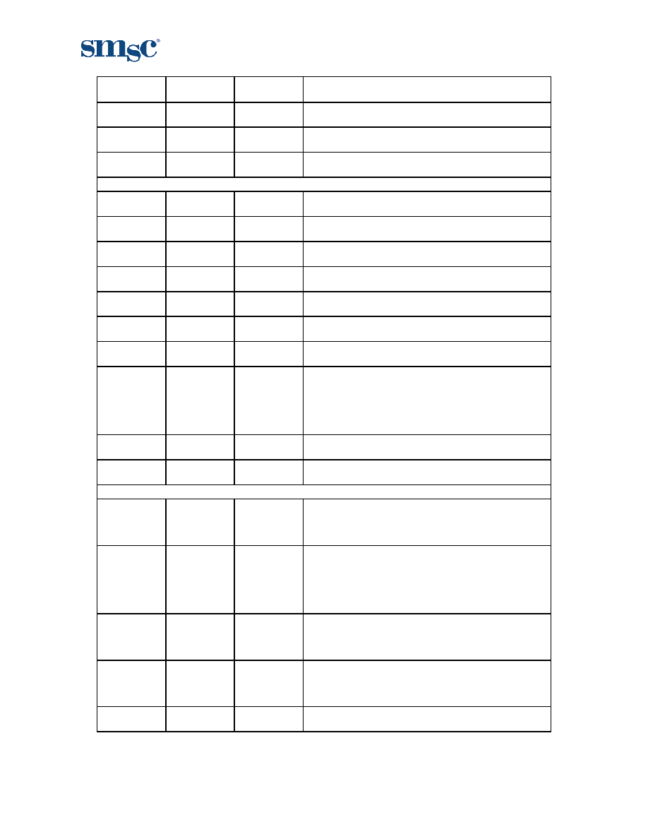
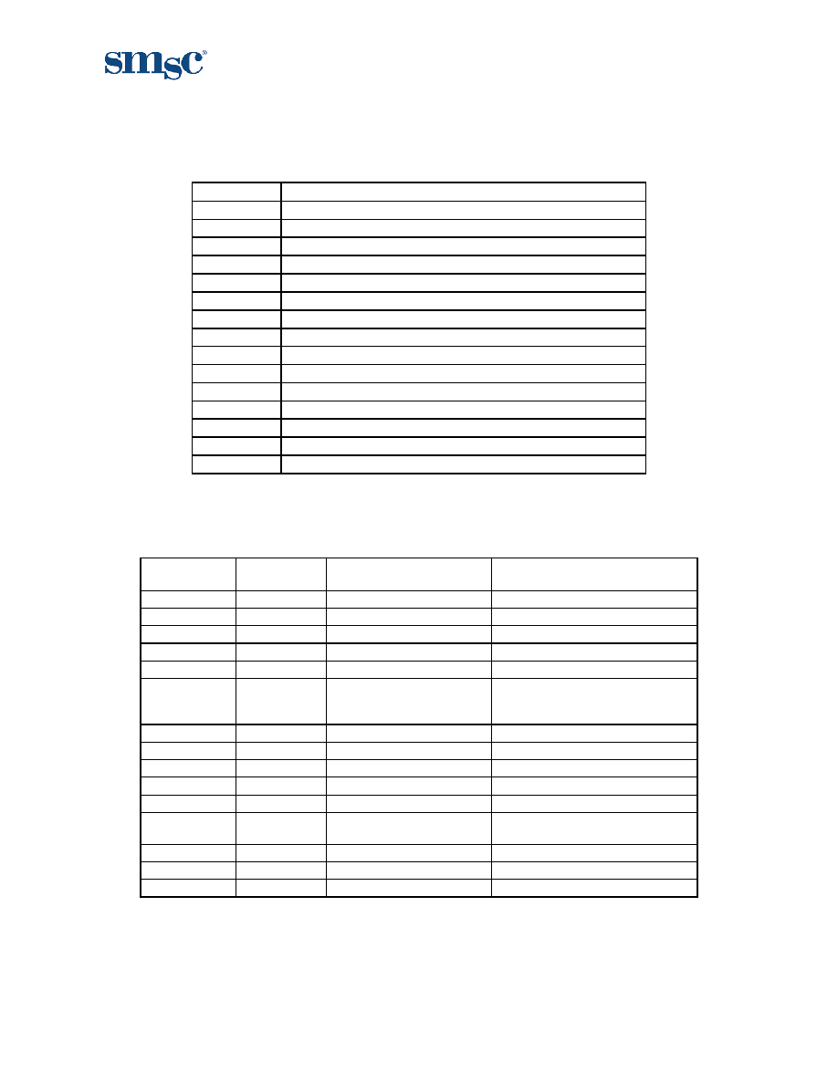
Chapter 3 Pin Table
3.1 128-Pin
Package
Table 3.1 - Pinout
CompactFlash INTERFACE (28 Pins)
CF_D0 CF_D1 CF_D2
CF_D3
CF_D4 CF_D5 CF_D6
CF_D7
CF_D8 CF_D9 CF_D10
CF_D11
CF_D12 CF_D13 CF_D14
CF_D15
CF_nIOR CF_nIOW CF_IRQ
CF_nRESET
CF_IORDY CF_nCS0 CF_nCS1 CF_SA0
CF_SA1 CF_SA2 CF_nCD1
CF_nCD2
SmartMedia / XD INTERFACE (17 Pins)
SM_D0 SM_D1 SM_D2
SM_D3
SM_D4 SM_D5 SM_D6
SM_D7
SM_ALE SM_CLE SM_nRE
SM_nWE
SM_nWP SM_nB/R SM_nCE
SM_nCD
SM_nWPS
Memory Stick INTERFACE (7 Pins)
MS_BS MS_SDIO/MS_D0
MS_SCLK MS_INS
MS_D1 MS_D2 MS_D3
SD INTERFACE (7 Pins)
SD_CMD SD_CLK SD_DAT0
SD_DAT1
SD_DAT2 SD_DAT3 SD_nWP
USB INTERFACE (13 Pins)
USB+ USB- ATEST
RBIAS
VDDP VSSP
(2)VDDA
(2)VSSA
VREG XTAL1/CLKIN XTAL2
MEMORY/IO INTERFACE (27 Pins)
MA0 MA1 MA2
MA3
MA4 MA5 MA6
MA7
MA8 MA9 MA10
MA11
MA12 MA13 MA14
MA15
MD0 MD1 MD2
MD3
MD4 MD5 MD6
MD7
nMRD nMWR nMCE
MISC (18 Pins)
nRESET GPIO1 GPIO2 GPIO3
GPIO4 GPIO5
GPIO6/ROMEN GPIO7
GPIO8 GPIO9 GPIO10
GPIO11
GPIO12 GPIO13 GPIO14
GPIO15
nTEST0 nTEST1
DIGITAL, POWER, GROUND & NC (11 Pins)
(3)VDDIO (4)VSSIO
(2)VDDCORE
(2)VSSCORE
Total 128
Bus Powered USB 2.0 Flash Media Controller
Datasheet
Revision 1.4 (08-27-03)
Page 8
SMSC USB97C223
DATASHEET
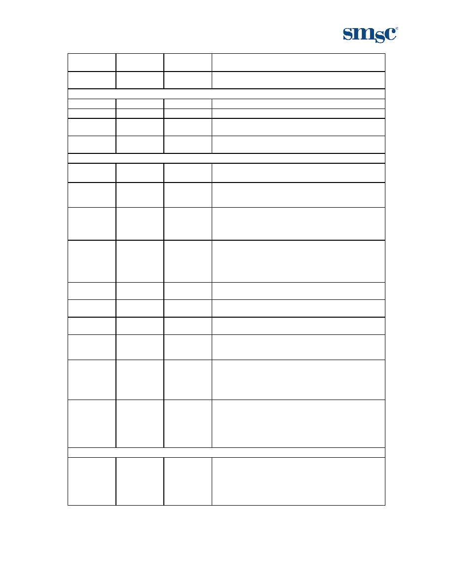
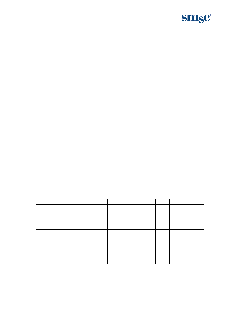
3.2
128 Pin List Table
3.2.1 128 Pin TQFP
PIN #
NAME
MA PIN #
NAME
MA PIN #
NAME
MA PIN #
NAME
MA
1 MA0
8
33 MS_D2
8
65 CF_nCD2
-
97 ATEST
-
2
MA1
8 34
MS_D1
8 66
CF_IRQ
- 98
VDDP
3 MA2
8
35 MS_D0
8
67 CF_IORDY
-
99 XTAL2
-
4
VDDIO
36 MS_SCLK
8
68 CF_nIOR
8 100 XTAL1
-
5
MA3
8 37
MS_BS
8 69
CF_nIOW
8 101
VSSP
6 MA4
8
38 SD_nWP
-
70 CF_nRESET
8 102 VDDA(REF)
7 MA5
8 39 VDDIO
71
CF_nCS0
8 103
RBIAS
-
8
MA6
8 40
SD_DAT0
8 72
CF_nCS1
8 104
VSSA(REF)
9
MA7
8 41
SD_DAT1
8 73
CF_SA0
8 105
VDDA
10 MA8
8
42 SD_DAT2
8
74 VDDIO
106
USB+
-
11 MA9
8
43 SD_DAT3
8
75 CF_SA1
8 107 USB-
-
12 MA10
8
44 SD_CMD
8
76 CF_SA2
8 108 VSSA
13 MA11
8
45 SD_CLK
8
77 SM_D0
8 109 nRESET
-
14 MA12
8 46
CF_D0
8 78
SM_D1
8 110
VSSCORE
15 MA13
8 47
CF_D1
8 79
VSSIO
111
nTEST0
-
16 VDDCORE
48 CF_D2
8
80 SM_D2
8 112 nTEST1
-
17 MA14
8
49 CF_D3
8
81 SM_D3 8
113
GPIO1 8
18 MA15
8
50 CF_D4
8
82 SM_D4
8 114 GPIO2
8
19 MD0
8
51 VSSIO
83
SM_D5
8 115
GPIO3
8
20 MD1
8
52 VSSCORE
84
SM_D6
8
116
GPIO4
8
21 MD2
8
53 CF_D5
8
85 SM_D7
8 117 GPIO5
8
22 MD3
8
54 CF_D6
8
86 SM_ALE
8 118 GPIO6/ROMEN 8
23 VSSIO
55 CF_D7
8
87 SM_CLE
8 119 GPIO7
8
24 MD4
8 56
CF_D8
8 88
SM_nRE
8 120
GPIO8
8
25 MD5
8
57 CF_D9
8
89 SM_nWE
8 121 GPIO9
8
26 MD6
8
58 CF_D10
8
90 SM_nWP
8 122 GPIO10
8
27 MD7
8 59
CF_D11
8 91
VDDCORE
123
GPIO11
8
28 nMRD
8
60 CF_D12
8 92
SM_nCE
8 124
VSSIO
29 nMWR
8
61 CF_D13
8
93 VREG
125
GPIO12
8
30 nMCE
8
62 CF_D14
8
94 SM_nWPS
- 126 GPIO13
8
31 MS_INS
-
63 CF_D15
8
95 SM_nB/R
- 127 GPIO14
8
32 MS_D3
8
64 CF_nCD1
-
96 SM_nCD
- 128 GPIO15
8
Note 1:
RBIAS is connected to the Analog Ground plane VSSA(REF) via a resistor.
Note 2: When the internal 1.8V regulator is enabled, VDDCORE (91) and VDDP(98), MUST have a 10uf +/- 20%,
(equivalent series resistance (ESR) <0.1ohm) bypass capacitor to VSSA.
Note 3:
VDDA(REF) and VSSA(REF) are same as the VDDA and VSSA respectively.
Bus Powered USB 2.0 Flash Media Controller
Datasheet
SMSC USB97C223
Page 9
Revision 1.4 (08-27-03)
DATASHEET
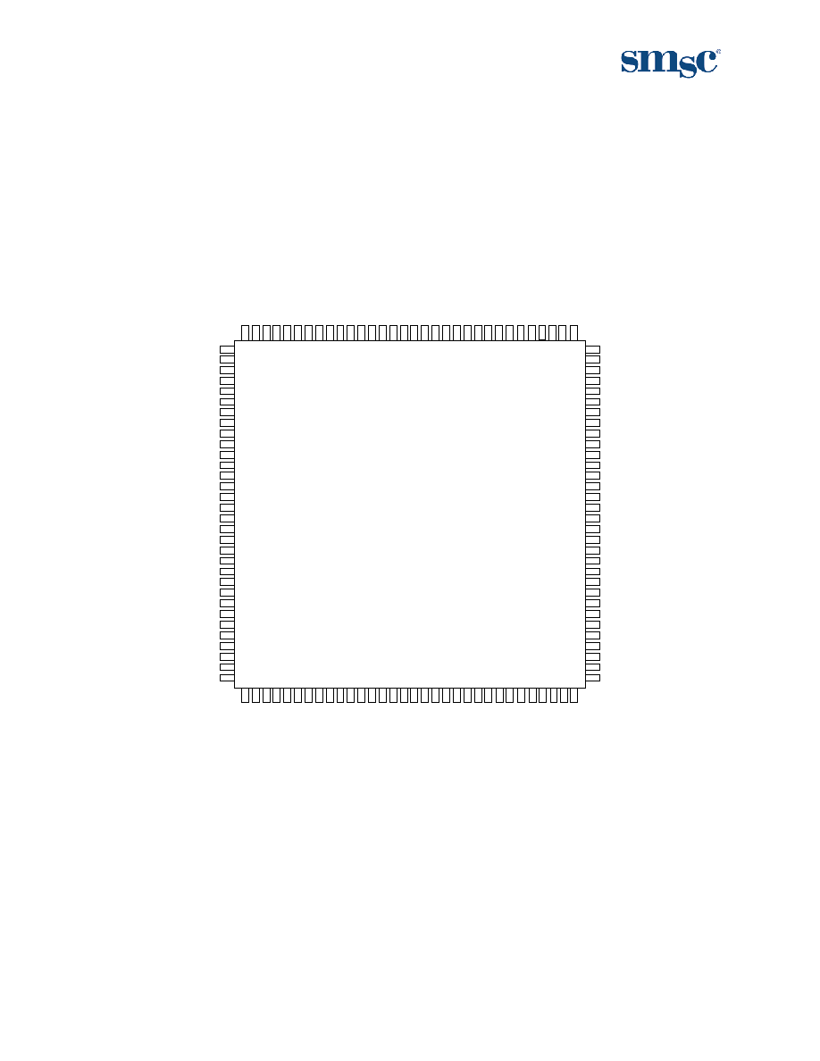
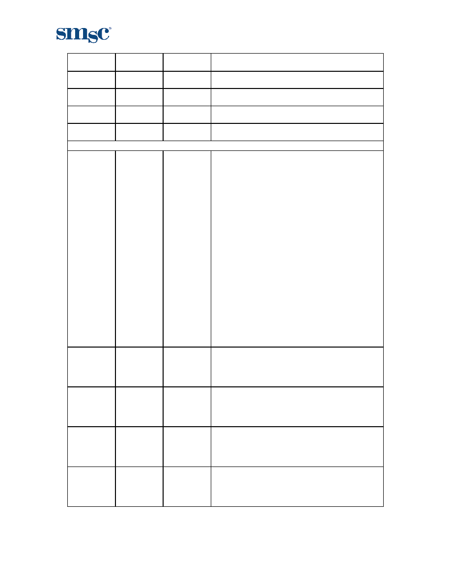
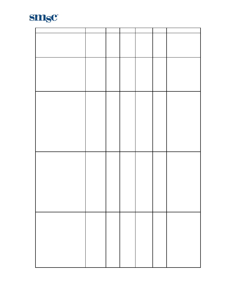
Chapter 4 Pin Configuration
4.1
128 Pin TQFP
GP
I
O
1
5
GP
I
O
1
4
GP
I
O
1
3
GP
I
O
1
2
VS
SI
O
GP
I
O
1
1
GP
I
O
1
0
GP
I
O
9
GP
I
O
8
GP
I
O
7
GP
I
O
6
/
ROME
N
GP
I
O
5
GP
I
O
4
GP
I
O
3
GP
I
O
2
GP
I
O
1
nTE
S
T1
nTE
S
T0
VS
SCO
R
E
n
R
ES
ET
VS
SA
USB
-
USB
+
VDDA
VS
SA
(RE
F
)
RBI
A
S
VDDA
(RE
F
)
VS
SP
XTA
L
1
XTA
L
2
VDDP
ATE
S
T
MS
_D2
MS
_D1
MS
_D0
MS
_S
CLK
MS_
B
S
SD
_
n
W
P
VDD
I
O
SD_
D
AT0
SD_
D
AT1
SD_
D
AT2
SD_
D
AT3
SD_
C
MD
SD_
C
LK
CF_D0
CF_D1
CF_D2
CF_D3
CF_D4
V
SSI
O
V
SSC
O
R
E
CF_D5
CF_D6
CF_D7
CF_D8
CF_D9
CF_
D
10
CF_
D
11
CF_
D
12
CF_
D
13
CF_
D
14
CF_
D
15
CF_
n
CD1
USB97C223
32
64
96
1
MA0
MA1
MA2
VDDIO
MA3
MA4
MA5
MA6
MA7
MA8
MA9
MA10
MA11
MA12
MA13
VDDCORE
MA14
MA15
MD0
MD1
MD2
MD3
VSSIO
MD4
MD5
MD6
MD7
nMRD
nMWR
nMCE
MS_INS
MS_D3
SM_nCD
SM_nB/R
SM_nWPS
VREG
SM_nCE
VDDCORE
SM_nWP
SM_nWE
SM_nRE
SM_CLE
SM_ALE
SM_D7
SM_D6
SM_D5
SM_D4
SM_D3
SM_D2
VSSIO
SM_D1
SM_D0
CF_SA2
CF_SA1
VDDIO
CF_SA0
CF_nCS1
CF_nCS0
CF_nRESET
CF_nIOW
CF_nIOR
CF_IORDY
CF_IRQ
CF_nCD2
Bus Powered USB 2.0 Flash Media Controller
Datasheet
Revision 1.4 (08-27-03)
Page 10
SMSC USB97C223
DATASHEET
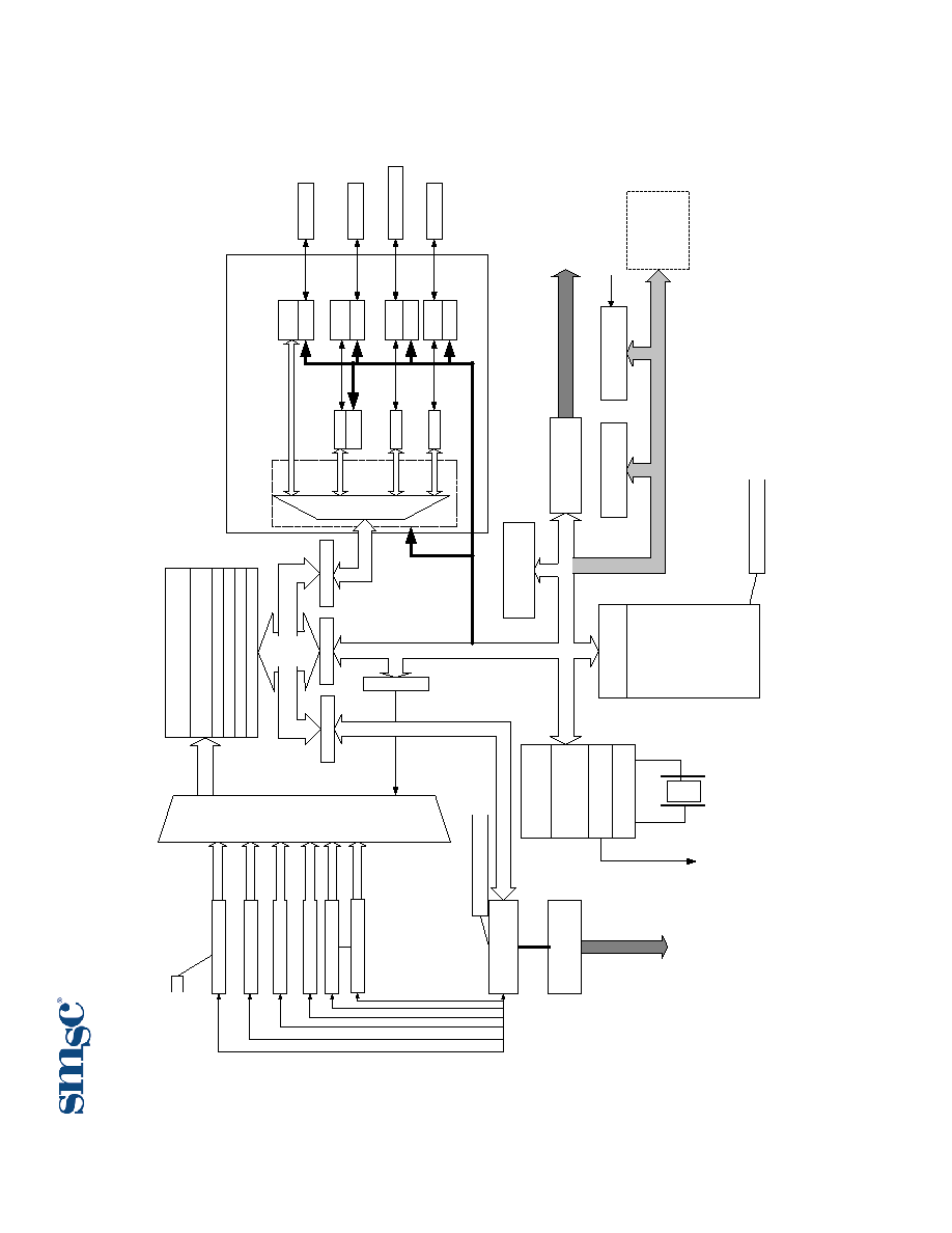
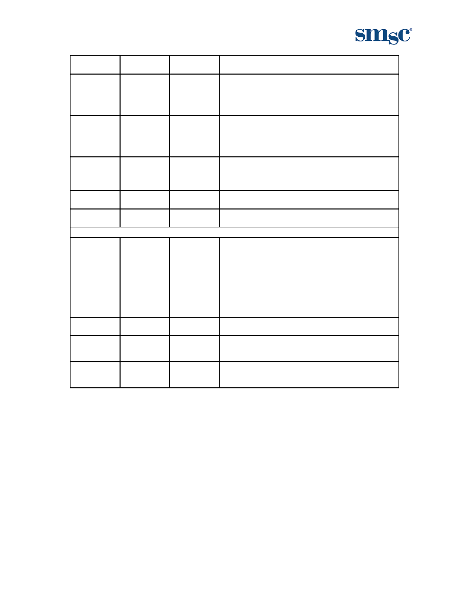
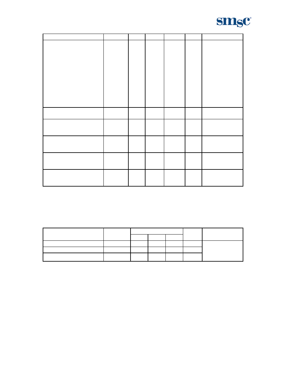
Chapter 5 Block Diagram
D
a
t
a
B
u
s
s
USB 2.0 PHY
( Transciever )
FAST 8051
CPU CORE
GPIO
15 pins
7 p
i
ns
Configuration and Control
Clock Generation
XTAL
SIE
( Serial Interface Engine )
Program Memory/ IO
Bus
Interrupt Controller
Latch phase 0, 2
SIE
Latch phase 3
8051
Latch phase 1
FMC
60MHz
32 Bit
Osc
Address
XD
AT
A
&
SF
R
Addr
e
s
s an
d Da
t
a
b
u
ss
e
s
64 Bytes EP0TX
64 Bytes EP0RX
64 Bytes EP1TX
64 Bytes EP1RX
Auto address generators
Addr
ess M
U
X
Data @ 32 bit
15Mhz
SIE Control Regs
Address
Address
Address
Address
EP0RX_BC
RAMRD_A/B
EP0TX_BC
RAMWR_A/B
32 bit 15MHz Data Buss
CLOCKOUT
12 MHz
512 Bytes EP2 TX/RX Buffer A
Addre
ss Regi
s
t
e
r
1.25KB
SRAM
12K Byte
Scratchpad
SRAM
Clocked byPhase 0, 2 Clock
Clocked by Phase 3 Clock
512 Bytes EP2 TX/RX Buffer B
Memory
Cards
Scratchpad
SRAM (768 Byte)
FM
C
Da
t
a
M
U
X
ECC
Control/
Status
SD
Controller
SD/MMC
Flash Media
Controllers
(FMC)
Control/
Status
MS
Controller
MS/HS MS/MS PRO
Control/
Status
SM
Controller
SM/SSFDC
Control/
Status
CF
Controller
CF
Control/
Status
CRC
MEM/IO Bus 29pins
DATA
DATA
DATA
DATA
CRC
EP1TX_BC
EP1RX_BC
Address
Address
Flash Media DMA Unit
64K ROM
ROMEN
Bus Powered USB 2.0 Flash Media Controller
Datasheet
SMSC USB97C223
Page 11
Revision 1.4 (08-27-03)
DATASHEET
Chapter 6 Pin Descriptions
This section provides a detailed description of each signal. The signals are arranged in functional groups
according to their associated interface.
The "n" symbol in the signal name indicates that the active, or asserted state occurs when the signal is at a
low voltage level. When "n" is not present before the signal name, the signal is asserted when at the high
voltage level.
The terms assertion and negation are used exclusively. This is done to avoid confusion when working with
a mixture of "active low" and "active high" signal. The term assert, or assertion indicates that a signal is
active, independent of whether that level is represented by a high or low voltage. The term negate, or
negation indicates that a signal is inactive.
6.1 Pin
Descriptions
Table 6.1 - Pin Description
NAME SYMBOL
BUFFER
TYPE
DESCRIPTION
CompactFlash (In True IDE mode) INTERFACE
CF Chip Select
1
CF_nCS1
O8
This pin is the active low chip select 1 signal for the CF
ATA device
CF Chip Select
0
CF_nCS0
O8
This pin is the active low chip select 0 signal for the task
file registers of CF ATA device in the True IDE mode.
CF Register
Address 2
CF_SA2
O8
This pin is the register select address bit 2 for the CF
device.
CF Register
Address 1
CF_SA1
O8
This pin is the register select address bit 1 for the CF
device.
CF Register
Address 0
CF_SA0
O8
This pin is the register select address bit 0 for the CF
device.
CF Interrupt
CF_IRQ
IPD
This is the active high interrupt request signal from the CF
device.
CF Data 15-8
CF_D[15:8] I/O8
The
bi-directional data signals CF_D15-CF_D8 in True
IDE mode data transfer. The bi-directional data signal has
an internal weak pull-down resistor.
CF Data7-0
CF_D[7:0]
I/O8
The bi-directional data signals CF_D7-CF_D0 in the True
IDE mode data transfer.
In the True IDE Mode, all of task file register operation
occur on the CF_D[7:0], while the data transfer is on
CF_D[15:0].
The bi-directional data signal has an internal weak pull-
down resistor.
IO Ready
CF_IORDY
IPU
This pin is active high input signal from CF card.
CF Card
Detection2
CF_nCD2
IPU
This card detection pin is connected to the ground on the
CF device, when the CF device is inserted.
CF Card
Detection1
CF_nCD1 IPU
This card detection pin is connected to ground on the CF
device, when the CF device is inserted.
Bus Powered USB 2.0 Flash Media Controller
Datasheet
Revision 1.4 (08-27-03)
Page 12
SMSC USB97C223
DATASHEET
NAME SYMBOL
BUFFER
TYPE
DESCRIPTION
CF Hardware
Reset
CF_nRESET
O8
This pin is an active low hardware reset signal to CF
device.
CF IO Read
CF_nIOR
O8
This pin is an active low read strobe signal for CF device,
when the CFC is enabled.
CF IO Write
Strobe
CF_nIOW
O8
This pin is an active low write strobe signal for CF device,
when the CFC is enabled.
SmartMedia INTERFACE
SM Write
Protect
SM_nWP
O8
This pin is an active low write protect signal for the SM
device, when the SMC is enabled.
SM Address
Strobe
SM_ALE
O8
This pin is an active high Address Latch Enable signal for
the SM device, when the SMC is enabled.
SM Command
Strobe
SM_CLE
O8
This pin is an active high Command Latch Enable signal
for the SM device, when the SMC is enabled.
SM Data7-0
SM_D[7:0]
I/O8
These pins are the bi-directional data signal SM_D7-
SM_D0, when the SMC is enabled.
SM Read
Enable
SM_nRE
O8
This pin is an active low read strobe signal for SM device,
when SMC is enabled.
SM Write
Enable
SM_nWE
O8
This pin is an active low write strobe signal for SM device,
when SMC is enabled.
SM Write
Protect Switch
SM_nWPS
IPU
A write-protect seal is detected, when this pin is low.
SM Busy or
Data Ready
SM_nB/R
I
This pin is connected to the BSY/RDY pin of the SM
device.
An external pull-up resistor is required on this signal. The
pull-up resistor should be attached to the power of
SM/NAND flash device.
SM Chip
Enable
SM_nCE
O8
This pin is the active low chip enable signal to the SM
device.
SM Card
Detection
SM_nCD
IPU
This is the card detection signal from SM device to
indicate if the device is inserted.
MEMORY STICK INTERFACE
MS Bus State
MS_BS
O8
This pin is connected to the BS pin of the MS device.
It is used to control the Bus States 0, 1, 2 and 3 (BS0,
BS1, BS2 and BS3) of the MS device.
MS System
Data In/Out
MS_SDIO
/MS_D0
I/O8
This pin is a bi-directional data signal for the MS device.
Most significant bit (MSB) of each byte is transmitted first
by either MSC or MS device.
The bi-directional data signal has an internal weak pull-
down resistor.
MS System
Data In/Out
MS_D1
IO8PD
This pin is a bi-directional data signal for the MS device.
The bi-directional data signal has an internal weak pull-
down resistor that is internally controlled.
MS System
Data In/Out
MS_D[3:2]
I/O8
This pin is a bi-directional data signal for the MS device.
The bi-directional data signal has an internal weak pull-
down resistor.
MS Card
Insertion
MS_INS
IPU
This pin is the card detection signal from the MS device to
indicate, if the device is inserted.
Bus Powered USB 2.0 Flash Media Controller
Datasheet
SMSC USB97C223
Page 13
Revision 1.4 (08-27-03)
DATASHEET
NAME SYMBOL
BUFFER
TYPE
DESCRIPTION
MS System
CLK
MS_SCLK
O8
This pin is an output clock signal to the MS device.
SD INTERFACE
SD Data3-0
SD_DAT[3:0]
I/O8
These are bi-directional data signals.
SD Clock
SD_CLK
O8
This is an output clock signal to SD/MMC device.
SD Command
SD_CMD
I/O8
This is a bi-directional signal that connects to the CMD
signal of SD/MMC device.
SD Write
Protected
SD_nWP
IPD
This pin is Write Protect Switch input signal with an
internal weak pull-down.
USB INTERFACE
USB Bus Data
USB-
USB+
IO-U
These pins connect to the USB bus data signals.
USB
Transceiver
Bias
RBIAS I
A 12.0K
± 1% resistor is attached from ground to this
pin to set the transceiver's internal bias currents.
Analog Test
ATEST
IOA
This signal is used for testing the analog section of the
chip and for enabling and disabling the internal 1.8 volt
regulator. This pin should be connected to VDDA to
enable the internal regulator or to VSSA to disable it.
1.8v Analog
Power
VDDP
1.8v Analog Power
If the internal 1.8V regulator is enabled, this pin MUST
have a 10uf +/- 20%, (equivalent series resistance (ESR)
<0.1ohm) bypass capacitor to VSSA. This capacitor
should be placed as close to the pin as possible.
Analog Ground
Reference
VSSP
Analog Ground Reference for 1.8v Analog power.
3.3v Analog
Power
VDDA
3.3v Analog Power
Analog Ground
Reference
VSSA
Analog Ground Reference for 3.3v Analog Power.
1.8v Voltage
Regulator for
USB PHY
VREG
This pin is connected to 3.3v.
Crystal
Input/External
Clock Input
XTAL1/
CLKIN
ICLKx
12Mhz Crystal or external clock input.
This pin can be connected to one terminal of the crystal
or can be connected to an external 12Mhz clock when a
crystal is not used.
Crystal Output
XTAL2
OCLKx
12Mhz Crystal
This is the other terminal of the crystal, or left open when
an external clock source is used to drive XTAL1/CLKIN.
It may not be used to drive any external circuitry other
than the crystal circuit.
MEMORY/IO INTERFACE
Memory Data
Bus
MD[7:0]
IO8
When using external program memory, these signals are
used to transfer data between the internal CPU and the
external program memory.
When using internal program ROM, internal weak pull up
resistors are activated to prevent these pins from floating.
Bus Powered USB 2.0 Flash Media Controller
Datasheet
Revision 1.4 (08-27-03)
Page 14
SMSC USB97C223
DATASHEET
NAME SYMBOL
BUFFER
TYPE
DESCRIPTION
Memory
Address Bus
MA[15:0]
O8
These signals address memory locations within the
external memory.
Memory Read
Strobe
nMWR
O8
Program Memory Write; active low
Memory Read
Strobe
nMRD
O8
Program Memory Read; active low
Memory Chip
Enable
nMCE
O8
Program Memory Chip Enable; active low. This signal is
asserted, when the device is not is SUSPEND mode.
MISC
GPIO6,
ROMEN and
RXD
GPIO6
/ROMEN
I/O8PU
This pin has an internal weak pullup resistor that can be
enabled or disabled by the state of nRESET.
The pullup is enabled when nRESET is active.
The pullup is disabled, when the nRESET is inactive
(some clock cycles later, after the rising edge of
nRESET).
The state of this pin is latched internally on the rising
edge of nRESET to determine if internal or external
program memory is used.
The state latched is stored in ROMEN bit of GPIO_IN1
register. After the rising edge of nRESET, this pin may be
used as GPIO6 or RXD.
When pulled low via an external weak pulldown resistor,
an external program memory should be connected to the
memory data bus. The USB97C223 uses this external
bus for program execution.
When this pin is left unconnected or pulled high by a
weak pullup resistor, the USB97C223 uses the internal
ROM for program execution.
This pin's function while operating from internal ROM is
shown in Section 6.3 , GPIO Usage.
General
Purpose I/O
GPIO1
I/O8
This pin may be used either as input, edge sensitive
interrupt input, or output.
This pin's function while operating from internal ROM is
shown in Section 6.3 , GPIO Usage.
General
Purpose I/O
GPIO2
I/O8
This pin may be used either as input, edge sensitive
interrupt input, or output.
This pin's function while operating from internal ROM is
shown in Section 6.3 , GPIO Usage.
General
Purpose I/O
GPIO3
I/O8
This pin may be used either as input, edge sensitive
interrupt input, or output.
This pin's function while operating from internal ROM is
shown in Section 6.3 , GPIO Usage.
General
Purpose I/O
GPIO4
I/O8
This pin may be used either as input, edge sensitive
interrupt input, or output.
This pin's function while operating from internal ROM is
shown in Section 6.3 , GPIO Usage.
Bus Powered USB 2.0 Flash Media Controller
Datasheet
SMSC USB97C223
Page 15
Revision 1.4 (08-27-03)
DATASHEET
NAME SYMBOL
BUFFER
TYPE
DESCRIPTION
General
Purpose I/O
GPIO5
I/O8
This pin may be used either as input, edge sensitive
interrupt input, or output.
This pin's function while operating from internal ROM is
shown in Section 6.3 , GPIO Usage.
General
Purpose I/O
GPIO7
I/O8
This pin may be used either as input, edge sensitive
interrupt input, or output.
This pin's function while operating from internal ROM is
shown in Section 6.3 , GPIO Usage.
General
Purpose I/O
GPIO[15:8]
I/O8
These pins may be used either as input, or output.
These pins' functions while operating from internal ROM
are shown in Section 6.3 , GPIO Usage.
RESET input
nRESET
IS
This active low signal is used by the system to reset the
chip. The active low pulse should be at least 1
µs wide.
TEST Input
nTEST[0:1]
IPU
These signals are used for testing the chip. User should
normally tie them high externally.
DIGITAL POWER, GROUNDS, and NO CONNECTS
1.8v Digital
Core Power
VDDCORE
+1.8V Core power
All VDDCORE pins must be connected together on the
circuit board.
If the internal 1.8V regulator is enabled, pin 91 MUST
have a 10uf +/- 20%, (equivalent series resistance (ESR)
<0.1ohm) bypass capacitor to VSSA, and this capacitor
should be placed as close to the pin as possible.
3.3v Digital I/O
power
VDDIO
+3.3V I/O power
VDDCORE
reference
ground
VSSCORE
VDDCORE ground Reference
VDDIO
reference
ground
VSSIO
VDDIO ground reference
Note 1:
Hot-insertion capable card connectors are required for all of flash medias. It is required for SD connector to
have Write Protect switch. This allows the chip to detect MMC card.
Note 2: nMCE is normally asserted except when the system is in standby mode.
Bus Powered USB 2.0 Flash Media Controller
Datasheet
Revision 1.4 (08-27-03)
Page 16
SMSC USB97C223
DATASHEET
6.2
Buffer Type Descriptions
Table 6.2 - USB97C223 Buffer Type Descriptions
BUFFER DESCRIPTION
I Input
IPU
Input with controlled internal weak pull-up resistor.
IPD
Input with controlled internal weak pull-down resistor.
IS
Input with Schmitt trigger
I/O8
Input/Output with 8mA drive
I/OD8
Input/Open drain output ... 8mA sink
O8
Output with 8mA drive
I/O8PU
Input/Output with 8mA drive controlled weak pull-up resistor
I/O8PD
Input/Output with 8mA drive controlled weak pull-down resistor
ICLKx
XTAL clock input
OCLKx
XTAL clock output
I/O-U
Analog Input/Output Defined in USB specification
O-U Analog
Output
I-U Analog
Input
OIA
Special analog Input/Output
6.3
GPIO Usage Table
Table 6.3 - GPIO Usage ( ROM Rev 0x00)
NAME
ACTIVE
LEVEL
SYMBOL
DESCRIPTION AND NOTE
GPIO1
H
Unused
Unused output; NC
GPIO2 H
EE_CS
Serial
EE PROM chip select
GPIO3
H
V_BUS
USB V bus detect
GPIO4
H
EE_DIN/EE_DOUT
Serial EE PROM input/output
GPIO5
H
HS Ind.
High Speed USB indicator
GPIO6
H
A16 ( external ROM only )
/ROMEN
Int/Ext ROM select. External
program memory A16 address line
connect for DFU.
GPIO7
H
EE_CLK
Serial EE PROM clock output
GPIO8
L
MS Power Control
Memory Stick Card Power Control
GPIO9
L
CF Power Control
CompactFlash Card Power Control
GPIO10
L
SM Power Control
SmartMedia Card Power Control
GPIO11
L
SD Power Control
SD/MMC Card Power Control
GPIO12
H
MS/MSPro Activity
Memory Stick(/Pro) Activity
Indicator
GPIO13 H
CF
Activity
CompactFlash Activity Indicator
GPIO14
H
SM/XDActivity
SmartMedia/XD Activity Indicator
GPIO15 H
SD/MMC
Activity
SD/MMC Activity Indicator
Bus Powered USB 2.0 Flash Media Controller
Datasheet
SMSC USB97C223
Page 17
Revision 1.4 (08-27-03)
DATASHEET
Chapter 7 DC Parameters
7.1
Maximum Guaranteed Ratings
Operating Temperature Range .................................................................................................. 0
o
C to +70
o
C
Storage Temperature Range .................................................................................................. -55
o
to +150
o
C
Lead Temperature Range (soldering, 10 seconds) .............................................................................+325
o
C
Positive Voltage on any pin, with respect to Ground ............................................................................... 5.5V
Negative Voltage on any pin, with respect to Ground ............................................................................ -0.3V
Maximum V
DD,
V
DDP
.............................................................................................................................. +2.5V
Maximum V
DDIO,
V
DDA
............................................................................................................................ +4.0V
* Stresses above the specified parameters could cause permanent damage to the device. This is a stress
rating only and functional operation of the device at any other condition above those indicated in the
operation sections of this specification is not implied.
Notes:
When powering this device from laboratory or system power supplies, it is important that the Absolute Maximum
Ratings not be exceeded or device failure can result. Some power supplies exhibit voltage spikes on their
outputs when the AC power is switched on or off. In addition, voltage transients on the AC power line may
appear on the DC output. When this possibility exists, it is suggested that a clamp circuit be used.
The name "VDD" is the same as VDDCORE
7.2
DC Electrical Characteristics
(T
A
= 0∞C - 70∞C, V
DDIO,
V
DDA
= +3.3 V ± 10%, V
DD,
V
DDP
= +1.8 V ± 10%,)
PARAMETER SYMBOL
MIN
TYP
MAX
UNITS
COMMENTS
I Type Input Buffer
Low Input Level
High Input Level
V
ILI
V
IHI
2.0
0.8
V
V
TTL Levels
IS Type Input Buffer
Low Input Level
High Input Level
Hysteresis
V
ILI
V
IHI
V
HYSI
2.0
500
0.8
V
V
mV
TTL Levels
Bus Powered USB 2.0 Flash Media Controller
Datasheet
Revision 1.4 (08-27-03)
Page 18
SMSC USB97C223
DATASHEET
PARAMETER SYMBOL
MIN
TYP
MAX
UNITS
COMMENTS
ICLK Input Buffer
Low Input Level
High Input Level
V
ILCK
V
IHCK
2.2
0.4
V
V
Input Leakage
(All I and IS buffers)
Low Input Leakage
High Input Leakage
I
IL
I
IH
-10
-10
+10
+10
uA
mA
V
IN
= 0
V
IN
= V
DDIO
O8 Type Buffer
Low Output Level
High Output Level
Output Leakage
V
OL
V
OH
I
OL
2.4
-10
0.4
+10
V
V
uA
I
OL
= 8 mA @
V
DDIO
= 3.3V
I
OH
= -4mA @
V
DDIO
= 3.3V
V
IN
= 0 to V
DDIO
(Note 7.1)
I/O8 Type Buffer
Low Output Level
H
IGH
O
UTPUT
L
EVEL
Output Leakage
V
OL
V
OH
I
OL
2.4
-10
0.4
+10
V
V
µA
I
OL
= 8 mA @
V
DDIO
= 3.3V
I
OH
= -4 mA @
V
DDIO
= 3.3V
V
IN
= 0 to V
DDIO
(Note 7.1)
I/O12 Type Buffer
Low Output Level
High Output Level
Output Leakage
V
OL
V
OH
I
OL
2.4
-10
0.4
+10
V
V
µA
I
OL
= 12 mA @
V
DDIO
= 3.3V
I
OH
= -6mA @
V
DDIO
= 3.3V
V
IN
= 0 to V
DDIO
(Note 7.1)
Bus Powered USB 2.0 Flash Media Controller
Datasheet
SMSC USB97C223
Page 19
Revision 1.4 (08-27-03)
DATASHEET
PARAMETER SYMBOL
MIN
TYP
MAX
UNITS
COMMENTS
I/O24 Type Buffer
Low Output Level
High Output Level
Output Leakage
V
OL
V
OH
I
OL
2.4
-10
0.4
+10
V
V
µA
I
OL
= 24 mA @
V
DDIO
= 3.3V
I
OH
= -12 mA @
V
DDIO
= 3.3V
V
IN
= 0 to V
DDIO
(Note 7.1)
IO-U
(Note 7.2)
Supply Current Unconfigured
I
CCINIT
45
10
60
20
mA
mA
@ V
DD,
V
DDP
= 1.8V
@ V
DDIO,
V
DDA
=
3.3V
Supply Current Active
(Full Speed)
I
CC
35
15
60
30
mA
mA
@ V
DD,
V
DDP
= 1.8V
@ V
DDIO,
V
DDA
=
3.3V
Supply Current Active
(High Speed)
I
CC
45
15
70
30
mA
mA
@ V
DD,
V
DDP
= 1.8V
@ V
DDIO,
V
DDA
=
3.3V
Supply Current Standby
I
CSBY
160
215
180
240
µA
µA
@ V
DD,
V
DDP
= 1.8V
@ V
DDIO,
V
DDA
=
3.3V
Note 7.1
Output leakage is measured with the current pins in high impedance.
Note 7.2
See Appendix A for USB DC electrical characteristics.
CAPACITANCE T
A
= 25∞C; fc = 1MHz; V
DD,
V
DDP
= 1.8V
LIMITS
PARAMETER SYMBOL
MIN
TYP
MAX
UNIT
TEST
CONDITION
Clock Input Capacitance
C
IN
20
pF
Input Capacitance
C
IN
10
pF
Output Capacitance
C
OUT
20
pF
All pins except USB
pins (and pins
under test tied to
AC ground)
Bus Powered USB 2.0 Flash Media Controller
Datasheet
Revision 1.4 (08-27-03)
Page 20
SMSC USB97C223
DATASHEET
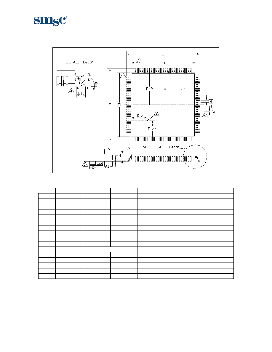
Chapter 8 Package Outline
Figure 8.1 - 128 Pin TQFP Package
Table 8.1 - 128 Pin TQFP Package Parameters
MIN NOMINAL MAX
REMARKS
A
~ ~
1.20
Overall
Package Height
A1
0.05 ~ 0.15
Standoff
A2
0.95 ~ 1.05
Body Thickness
D
15.80 ~ 16.20
X
Span
D1
13.80 ~ 14.20
X
body Size
E
15.80 ~ 16.20
Y
Span
E1
13.80 ~ 14.20
Y
body Size
H
0.09
~
0.20
Lead Frame Thickness
L
0.45
0.60
0.75
Lead Foot Length
L1
~ 1.00 ~
Lead
Length
e
0.40 Basic
Lead Pitch
0
o
~ 7
o
Lead Foot Angle
W
0.13 0.18 0.23
Lead
Width
R1
0.08
~
~
Lead Shoulder Radius
R2
0.08
~
0.20
Lead Foot Radius
ccc
~ ~
0.08
Coplanarity
Notes:
1) Controlling Unit: millimeter.
2) Tolerance on the true position of the leads is ± 0.035 mm maximum.
3) Package body dimensions D1 and E1 do not include the mold protrusion.
Maximum mold protrusion is 0.25 mm.
4) Dimension for foot length L measured at the gauge plane 0.25 mm above the seating plane.
5) Details of pin 1 identifier are optional but must be located within the zone indicated.